
Why we’re switching to Infrared for lead-free semiconductors
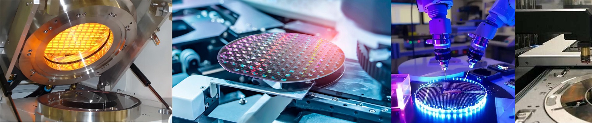
The semiconductor world is moving toward “lead-free” and “zero-emission” drying, and honestly, it’s about time. For years, we’ve relied on those massive convection ovens. They basically just heat up a giant box of air, which is a waste of power and—worst of all—risks blowing tiny particles right onto your wafers. That’s why we use infrared (IR) curing. Instead of heating the air, IR uses electromagnetic radiation to hit the substrate directly. No middleman. No hot air blowing around. Just direct energy.
The magic of IR energy
Here is how it actually works: we match the wavelength of the emitter to whatever coating or resist you’re using. In a lead-free setup, we stick with short-wave and medium-wave IR. It makes polymerization and solvent evaporation happen fast. Like,really fast. Think about it: a convection oven takes minutes just to get up to temp. Our IR setups? They hit the target in seconds. It changes the whole rhythm of the production line.
Keeping things clean (and cool)
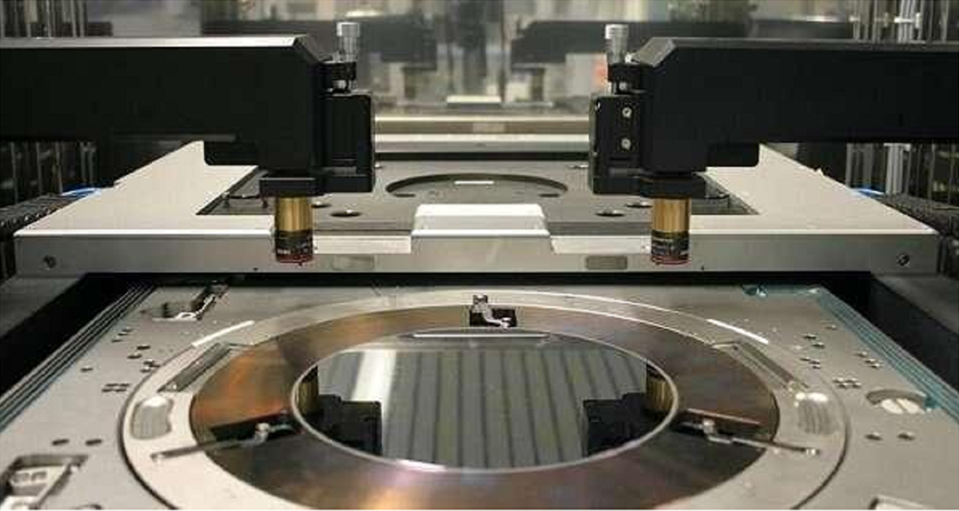
Since this has to work in a cleanroom, we build the heater housings out of high-grade stainless steel. We stay far away from plated materials because they tend to flake or off-gas, which is a nightmare for wafer quality. Plus, the stainless steel reflects that IR radiation right back toward the workpiece, so you aren’t losing heat into the chassis. But there’s a catch. High-density IR arrays get incredibly hot. If your airflow isn’t dialed in, the housing can warp or the whole system might just shut down to protect itself. To stop that from happening, we usually put forced-air cooling on the back of the housing. It keeps the footprint stable and the hardware happy.
Better for the planet, better for the bill
When you’re trying to get rid of lead and VOCs, you have to be careful. If you over-bake, you’ve ruined the batch. The beauty of IR is that you can use zoned heating. You can tweak one specific section of the curing line without having to heat up a massive oven. This knocks down your kilowatt-hour consumption per wafer significantly. It’s a much easier way to hit those ISO 14001 standards. You stop fighting the inertia of a giant hot box and finally start controlling the energy right where it matters.